Finally came to an end where I need to redesign the schematic again for lesser components and trying to get power source from FC rather from itself. The whole idea is to cut costs and able to build it easily. Below is the diagram currently I am working on and going to test out the firmware on BLHELI_s with the version O_H_5 but with some minor modification on the code. I had accidentally swapped the pins at the MOSFETs side. Lets see how it goes once the board is back from JLCPCB.
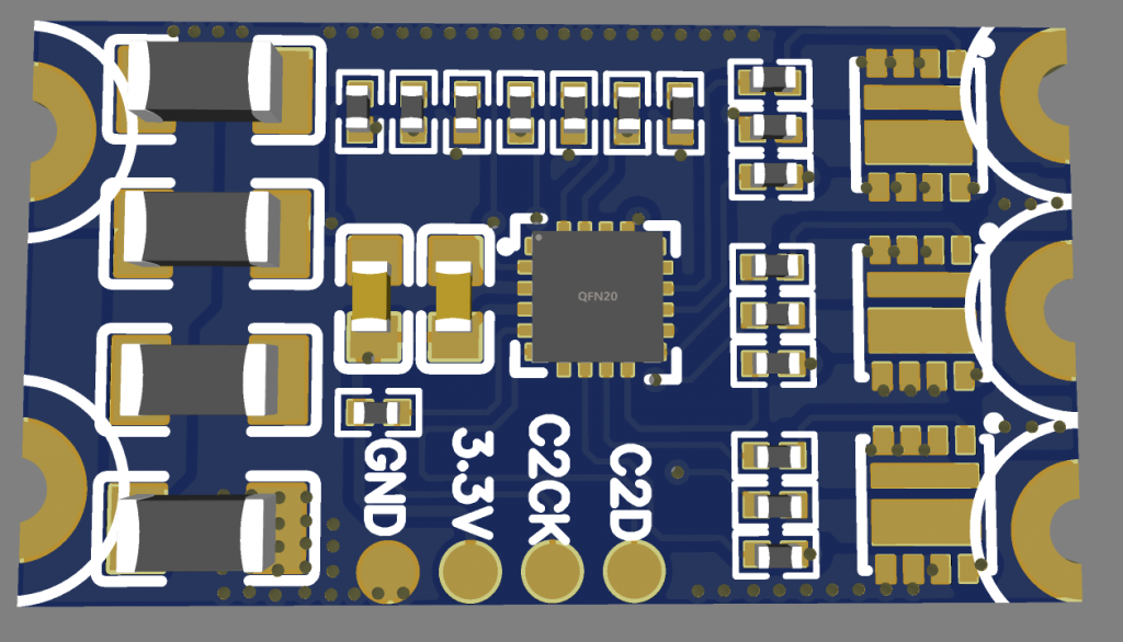
Below is the image of the ESC I had designed (Generated from EasyEDA):

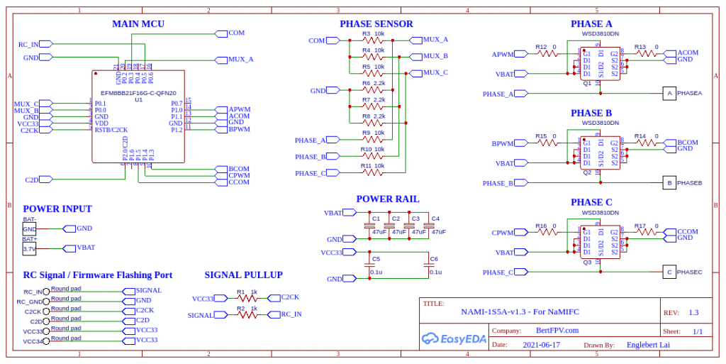
The Schematic:

As you can see, I am only using very little components here. Trying to make it as light as possible. Remember the power source for the ESC is from the FC. You need to build the FC with 3.3V and the raw power to drive the MOSFETs and motor.
The specification for this ESC design intended to run only on single cell and drain up to the lowest as possible. Below is the specifications of this design:
- Operating from 0.8v ~ 4.2v (Theoretically from the buck-booster chip that I am using at FC). I would predicted as it will be flat at 2.5v as the minimum it can go.
- Maximum rated 18A @ continuous and 45A @ pulsation mode.
- Maximum support protocol upto DSHOT600.
- Pass-Through mode supported through any FC. (Tested on INAV 3.0)
- PCB designed only 2-Layers.
- Only 1g for the weight of the ESC
- Initial flash from C2CK and C2D pins for loading the firmware into the EFM8BB21F16G.
Now for the time being, I will just wait for the components arrival and start testing it and sharing the details again once I get the result.